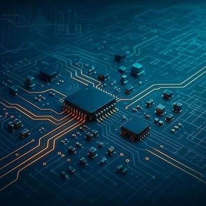
XDCPCBA is a leading supplier specializing in the manufacture and assembly of high-precision, high-quality PCBs, with expertise ranging from 2-layer PCB designing to complex 30-layer builds. We offer a diverse range including double-sided, multilayer, and flexible boards, making our products ideal for applications in communications, consumer electronics, security surveillance, industrial automation, the Internet of Things, medical electronics, rail transportation, automotive electronics, and aerospace—effectively meeting the unique needs of various industries. By utilizing advanced processes and state-of-the-art equipment, we ensure exceptional electrical performance and mechanical strength, with every stage of production undergoing rigorous inspection and testing. Furthermore, our professional assembly team and cutting-edge tools enable us to provide one-stop PCBA services, and by paying meticulous attention to detail—from precise component placement to superior soldering quality—we confidently handle complex requirements such as high-density assembly and micro-component placement, ultimately delivering reliable and stable PCBA products.
Key components 2 Layer PCB Designing
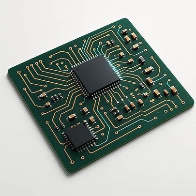
1. Essential Elements and Component Types
In a 2-layer PCB, designers use standard schematic symbols to represent major electronic components such as resistors, capacitors, inductors, diodes, transistors, and integrated circuits (ICs). They assign each component a footprint or package that defines the size and position of its electrical connection points on the board. These packages are generally classified into:
- THT (Through-Hole Technology) – Components with leads passing through the PCB, with connections accessible on all layers. For ICs, SIP and DIP packages are common.
- SMD (Surface Mount Devices) – Components mounted directly onto the PCB surface, typically on the top layer. IC packages include SOP, BGA, SOT-23, QFN, QFP, and SOT223, while passive components like resistors and capacitors come in sizes such as 01005, 0201, 0402, 0603, 0805, and beyond.
Other vital design elements include lines/connections, which represent electrical links between components—often labeled using net labels or annotations—and power sources and ground planes, which provide energy to the circuit. These high-current paths are usually designed with wider traces or polygon pours for improved conductivity.
2. Placement and Routing Guidelines for 2 Layer PCB Designing
For a 2-layer PCB, designers place components based on functionality, electrical parameters, power requirements, thermal considerations, and signal flow. They group components logically by function and position them to achieve the shortest feasible routing distances while maintaining signal integrity. Designers create conductive copper paths (traces) to interconnect components. They keep high-speed signal lines as short as possible to reduce signal degradation and interference, and they make high-current traces wider to lower resistance and voltage drop. They etch the copper layers precisely to form the required trace patterns, ensuring proper conductivity and isolation between adjacent paths.
Advantages of 2 Layer PCB Designing
- Cost-Effective and Efficient Manufacturing
- Enhanced Design Flexibility and Versatility
- Improved Electrical Performance Over Single-Layer Boards
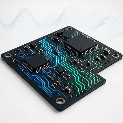
Applications of 2-Layer PCB Designing
Industries widely use 2-layer PCBs because they balance performance, cost, and versatility. Manufacturers commonly include them in consumer electronics, automotive systems, industrial equipment, and medical devices.:
Aerospace and Defense – Navigation units, control modules, and specialized monitoring equipment.
Consumer Electronics – Smartphones, audio devices, home appliances, and wearable technology.
Industrial Equipment – Control systems, automation devices, and power supplies.
Automotive Electronics – Instrument clusters, LED lighting systems, and infotainment modules.
Medical Devices – Portable diagnostic equipment, patient monitoring systems, and handheld instruments.
Communication Systems – Routers, modems, and network interface devices.
IoT Devices – Smart home products, environmental sensors, and wireless controllers.
Key Parameters in 2-Layer PCB Routing
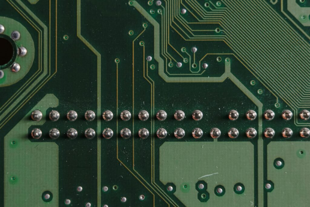
Inter-Layer Connectivity through Vias
In a 2-layer PCB, there is no defined stack-up as in multi-layer designs; instead, vias play a crucial role in connecting the top and bottom layers. Consequently, these plated holes not only enable component interconnections between layers but also allow traces to cross without interference.
Importing and Preparing the Circuit Design
Once the schematic—containing all circuit connections—is complete, it is imported into the PCB design file. From this point, designers can plan routing while keeping the layout compact and efficient.
Ensuring an Optimal Return Path
Furthermore, maintaining a clear and low-resistance return or ground path is essential to prevent power and signal integrity issues. A wider and more direct path enhances circuit performance.
Strategic Placement of Decoupling Capacitors
To improve stability, decoupling capacitors should be placed as close as possible to the IC power pins. As a result, they effectively stabilize power rails and filter high-frequency noise.
Grounding Techniques and Isolation
Additionally, grounding may need isolation depending on the circuit type—such as digital ground and analog ground. Techniques like star grounding, ground grids, and ground stitching can be used according to circuit requirements. However, excessive cuts or holes in power or ground planes can cause integrity problems.
Mechanical and Power Considerations
Mechanical factors, including connector positioning, casing, and box build, must also be addressed early in the design. Likewise, proper power distribution is vital to minimize voltage drops, noise, and fluctuations.
Effective Use of Silkscreen
Finally, the silkscreen layer is used to print component names, test point identifiers, connector labels, pin 1 indicators for ICs, and cathode markings for diodes. This not only aids assembly but also simplifies troubleshooting and maintenance.
Best Practices for Signal Integrity in 2 Layer PCB Designing
When working on 2-layer PCB designs, maintaining signal integrity requires careful planning of trace routing, component placement, and reference planes. Because there are fewer layers to work with compared to multi-layer boards, every design choice has a greater impact on performance. Therefore, it becomes essential to follow structured strategies that balance electrical performance with manufacturability.
Optimizing Power and Ground Distribution of 2 Layer PCB Designing
In a 2-layer PCB, achieving clean and stable power delivery requires both strategic trace planning and careful component placement. As shown above, placing decoupling capacitors close to power pins reduces voltage drops and noise. Wide copper traces or polygon pours should be used for both power and ground paths to minimize impedance. Additionally, connecting ground regions with multiple vias helps create a more uniform reference plane, which improves both signal integrity and EMI performance. Ultimately, every millimeter saved between power and ground return paths translates to a more robust and reliable circuit.
At Ampflick, we specialize in delivering high-quality 2-layer PCB designing services tailored to meet your exact requirements. With our expertise, advanced tools, and attention to detail, we ensure optimized layouts, reliable performance, and efficient production. Whether your project demands precision routing, superior signal integrity, or robust power distribution, Ampflick is your trusted partner for dependable and innovative 2-layer PCB solutions.
Visit our website Ampflick for more products.
You can also visit our Instagram and Facebook for latest update

