Zero PCB 12×18 cm Universal Board Single-Sided Price in Pakistan | AmpFlick
Original price was: ₨600.00.₨570.00Current price is: ₨570.00.
Delivered All over Pakistan 🇵🇰
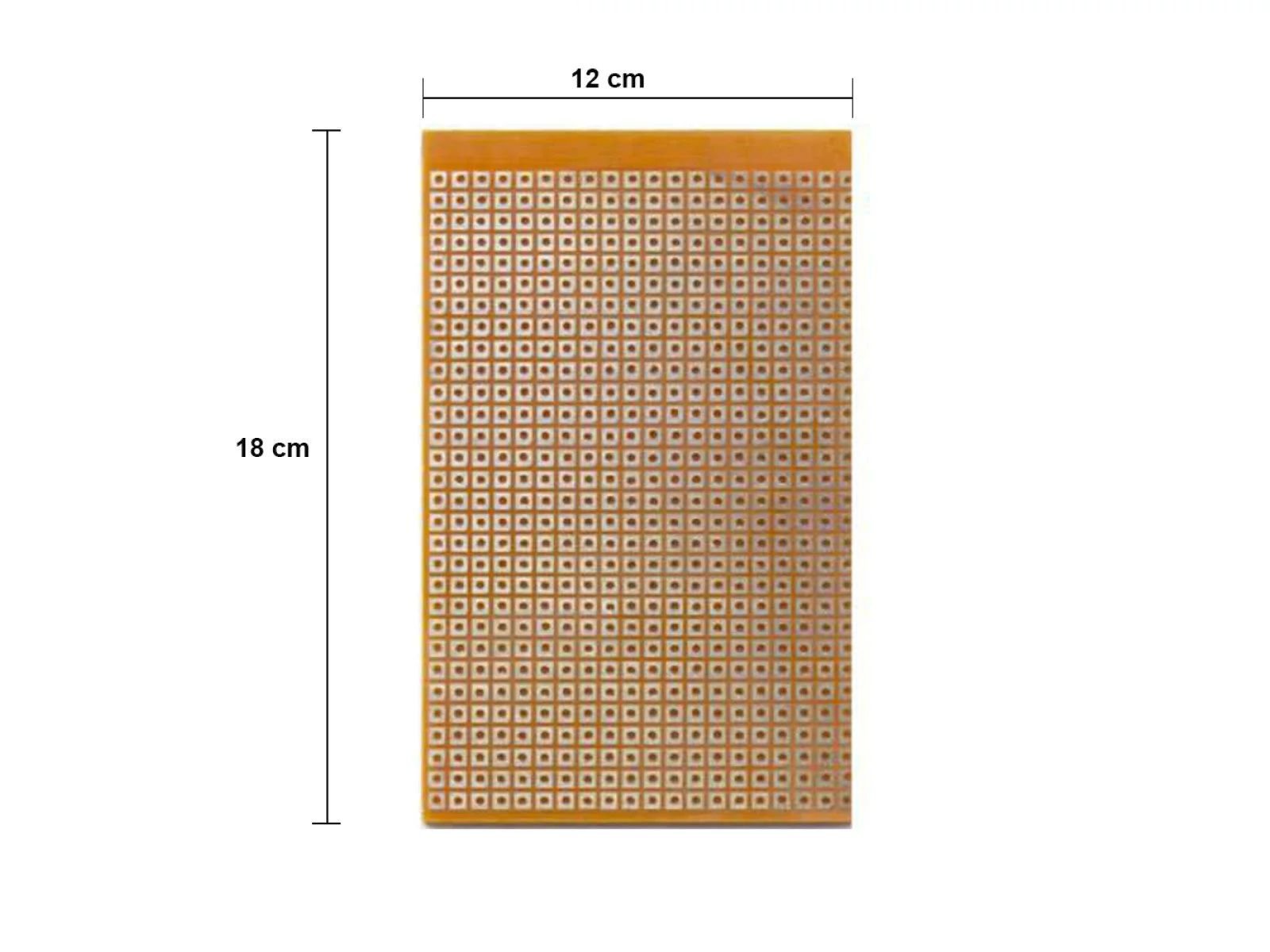
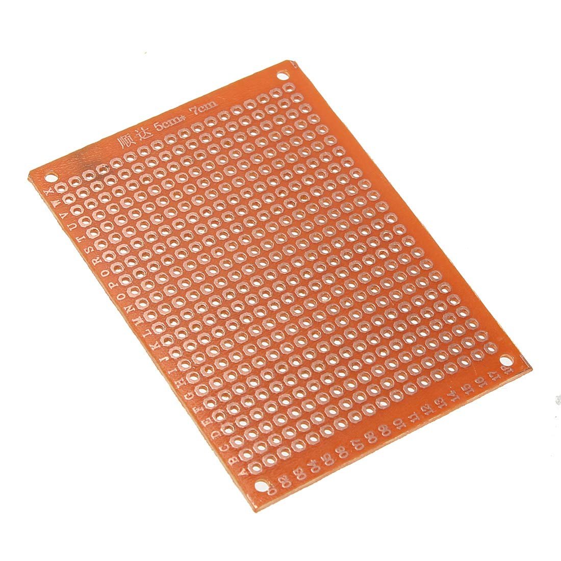
The Zero PCB 12×18 cm Universal Board is an essential multipurpose tool for electronic circuit design. It features a standard 2.54mm pitch across a spacious 12×18 cm copper-clad laminate. Specifically, the board includes printed coordinate markings to simplify the mapping of complex digital systems. The four corner mounting holes allow for stable integration into permanent project housings
Description
Professional 12×18 cm Single-Sided Universal Prototype Board
Technical Specifications of Zero PCB 12×18 cm Universal Board
-
Board Dimensions: Large 120mm by 180mm surface area for complex circuit integration.
-
Hole Pitch: Standard 2.54mm (0.1 inch) spacing compatible with all DIP integrated circuits.
-
Material: High-quality copper-clad laminated board featuring a single-sided conductive layer.
-
Pad Style: Pre-tinned round solder pads on the bottom for easy component bonding.
-
Layout Mapping: Printed rows and columns on the top side for organized pin identification.
-
Mounting: Four pre-drilled corner holes for secure chassis or standoff installation.
-
Keyphrase Usage: This Zero PCB 12×18 cm Universal Board provides a reliable permanent prototyping base.
Circuit Designing and Usage
-
First, align your electronic components according to the printed alphanumeric grid.
-
Next, insert the leads through the holes into the copper-padded bottom side.
-
Then, apply solder to create firm electrical connections between the leads and pads.
-
Afterward, utilize jumper wires or solder bridges to form the required circuit traces.
-
Consequently, the Zero PCB 12×18 cm Universal Board replaces messy temporary breadboard setups.
-
Finally, trim any excess board material using a PCB cutter for custom enclosure fitting.
Advantages and Disadvantages of Zero PCB 12×18 cm Universal Board
-
Pros: The massive 12×18 cm size accommodates large-scale robotics and industrial control projects.
-
Furthermore, the pre-tinned pads ensure excellent solder flow and high-conductivity joints.
-
Cons: Single-sided copper limits routing complexity compared to dual-layered plated through-hole boards.
-
Additionally, manual soldering of large matrices requires significant time and precision during assembly.
Precautions and Safety Guidelines
-
Warning: Always wear safety glasses when cutting or drilling the fiberglass laminate board.
-
Avoid overheating the copper pads to prevent them from peeling off the base material.
-
Ensure no solder bridges exist between adjacent pads to prevent accidental short circuits.
What is Included in the Package
-
1x Zero PCB 12×18 cm PCB Board (Single-Sided Copper Prototype Board).
-
Protective packaging to prevent oxidation of the copper pads during transit and storage.
Tutorial on how to use this: Click Here
Order more Prototyping Boards from AmpFlick: Click Here
🔗 Connect with the Ampflick Community
Stay updated with the latest hardware arrivals, project ideas, and engineering mentorship in Pakistan!
-
-
Instagram: @Ampflick — Daily project reels & hardware fashion.
-
LinkedIn: Ampflick Tech — Professional networking & career opportunities.
-
WhatsApp Support: Link to WhatsApp — Technical queries and bulk orders.
-
YouTube: Ampflick Official — Hardware masterclasses.
-
Only logged in customers who have purchased this product may leave a review.
Related products
-
-
Sale!
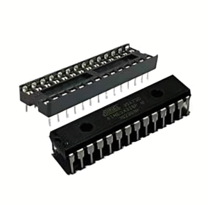
ATMEGA328P Chip
- Original price was: ₨900.00.₨855.00Current price is: ₨855.00.
- Add to cart
-
Sale!
Reviews
There are no reviews yet.