Introduction
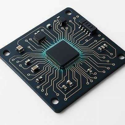
A printed circuit board, or PCB, is a key component in almost every electronic device. It connects and supports components using thin copper tracks. Instead of relying on wires, these copper paths allow signals and power to flow smoothly across the board. As a result, modern electronics are more compact, faster, and efficient. In many simple and cost-sensitive applications, Single Layer PCB Designing offers an ideal solution by using just one copper layer to achieve reliable circuit performance.
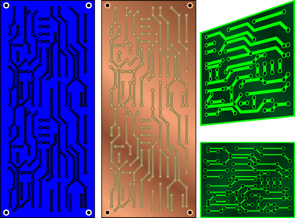
Among the different types of PCBs, a Single Layer PCB Designing also called a single-sided PCB—is the simplest. It has a conductive copper layer on one side, while the other side holds the components. Typically, these boards are made from materials such as paper-reinforced phenolic resin or glass fiber epoxy, both coated with copper foil.
Because of their basic structure, single-layer PCBs are easier to design and faster to produce. Therefore, they are often used in low-cost, low-density applications. For instance, they appear in devices like LED lights, calculators, and power supplies. However, their simplicity also brings limitations. Since there is only one layer, routing space is restricted. Consequently, they are not well suited for complex or high-speed circuits.
TYPES OF Single Layer PCB Designing
Single-layer PCBs can be designed in a few different ways depending on the material used, the complexity of the layout, and the application. Here are the most common types:
1. Rigid Single Layer PCB
Made from solid materials like fiberglass (FR4), these single-layer PCBs are by far the most commonly used type. Not only are they sturdy and durable, but they’re also highly cost-effective. As a result, they are widely used in everyday electronics such as calculators, LED lighting systems, and power supplies.
2. Flexible Single Layer PCB
These are built using flexible plastic substrates like polyimide. They can bend or twist, making them suitable for compact or foldable devices, such as cameras and wearable electronics.
3. High-Frequency Single Layer PCB
These are designed with materials that support high-frequency signals, such as Teflon. They’re often used in RF communication and satellite systems.
4. Aluminum-Based Single Layer PCB
These use aluminum as the base material for better heat dissipation. Commonly found in LED lighting and power conversion systems, they offer excellent thermal performance.
Advantages of Single Layer PCB Designing
Single-layer PCBs bring a wide range of benefits that make them an excellent choice for simple, low-cost electronic applications. Here are the key advantages you should know:
1. Simple and Easy to Design
To begin with, their straightforward layout makes it easy for designers—especially beginners—to create and organize circuits without unnecessary complexity.
2. Quick Assembly and Installation
Since all components go on one side, manufacturers can assemble and install the board quickly. This directly reduces production time and labor costs.
3. Reliable and Efficient
With only one conductive layer, designers eliminate many of the issues that come with multi-layer routing. As a result, the board becomes more stable and dependable in operation.
4. Faster Design Turnaround
Because the design process is less complicated, engineers can complete circuit layouts much faster. This speeds up development and helps meet tight project deadlines.
5. Reduced Risk of Electrical Noise or Short Circuits
By keeping the layout clean and simple, single-layer boards minimize the chances of interference or shorts, which often occur in more complex designs.
6. Cost-Effective for Mass Production
When it comes to large production runs, single-layer PCBs significantly lower manufacturing costs. Their basic structure requires fewer materials and less processing time compared to multi-layer alternatives.
7. Easier to Understand and Troubleshoot
Thanks to the visible and accessible layout, technicians can easily trace signal paths, identify faults, and fix issues without advanced tools or complicated analysis.
8. Minimal Use of Jumpers or Bridges
Since routing happens on one side, designers rarely need to use jumpers or zero-ohm resistors. This simplifies the layout and improves reliability.
9. Simplified Soldering and Component Insertion
Furthermore, tasks like drilling holes, inserting components, and soldering connections are easier and more efficient on single-layer boards.
10. Faster Maintenance and Repair
Finally, when issues arise, technicians can quickly inspect and repair the board without disassembling complex layers or navigating buried traces.
How to Design a Single Layer PCB Designing
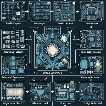
Designing a single-layer PCB involves a step-by-step process to ensure the board meets both electrical functionality and manufacturability. Here’s a streamlined guide to help you through it:
1. Schematic Capture
Begin by drawing your circuit using a schematic editor. Assign reference labels to each component (like R1 for resistors, C1 for capacitors, U1 for ICs, etc.). The schematic defines the electrical connections, which are exported as a netlist.
2. Assigning Footprints
Link each symbol in your schematic to its corresponding physical footprint (e.g., an 0805 SMD resistor or TO-92 package). Make sure pad sizes and hole diameters conform to manufacturing standards.
3. Initial Board Setup
Create a new PCB layout based on a single-layer template. Define the board’s dimensions and shape to match your project’s mechanical constraints.
4. Component Placement for Single Layer PCB Designing
Start by placing key components like connectors, microcontrollers, and power inputs. Then, arrange supporting components nearby to minimize trace lengths and avoid unnecessary interference.
5. Trace Routing
Since you’re working with only one conductive layer, route traces carefully. Keep enough spacing between them to prevent shorts. If trace crossings are unavoidable, consider using jumper wires or zero-ohm resistors—though they should be used sparingly.
6. Add Silkscreen Markings
First, label all components with reference designators and orientation indicators. Then, make sure to place the silkscreen text away from pads and holes so that the markings remain clear and readable after assembly.
7. Design Rule Check (DRC)
After completing your layout, run a DRC check using your PCB software. This step quickly identifies issues such as overlapping traces, tight clearances, or missing connections between pads. Fix all errors before moving forward.
8. Generate Gerber Files
Once the design is finalized, export your layout into Gerber files, including drill data, solder mask, and silkscreen layers. These files are essential for PCB manufacturing.
9. Manufacture or Prototype
Send the Gerber files to a PCB manufacturer. Be sure to confirm all details such as copper thickness, board material, surface finish, and via sizes.
How Single Layer PCBs Are Manufactured
Manufacturing a single-layer PCB involves a series of well-defined steps that ensure precision, durability, and optimal performance. Let’s walk through the process from start to finish:
1. Substrate Preparation
To begin with, manufacturers select a base material—typically fiberglass-reinforced epoxy (FR4). Next, they laminate a thin sheet of copper onto one side of this substrate, which then forms the foundation for the conductive layer of the PCB
2. Design Printing for Single Layer PCB Designing
Next, they apply a light-sensitive film, known as photoresist, over the copper surface. By exposing the board to UV light, they accurately imprint the circuit design onto the copper, clearly defining where the traces should remain.
3. Etching
After printing the design, manufacturers begin the etching process. They submerge the board in a chemical solution that removes the excess copper. Consequently, only the required copper paths that form the actual circuit remain.
4. Drilling
With the copper traces in place, the team drills holes at predefined locations to accommodate through-hole components. These drilled points are essential for mounting and soldering electronic parts.
5. Solder Mask Application
Following drilling, they apply a solder mask layer over the board. This step plays a crucial role—it protects the copper traces from oxidation and prevents unintended short circuits during assembly.
6. Silkscreen Printing
Then, they print helpful labels and symbols onto the board using silkscreen ink. This step adds part numbers, orientation markers, and branding elements, which greatly simplify assembly and maintenance.
.

Conclusion of Single Layer PCB Designing
Single-layer PCBs continue to be one of the most cost-effective and reliable solutions for basic electronic circuits. Whether you’re designing for consumer gadgets or industrial control systems, these boards stand out due to their simplicity, ease of design, and minimal production requirements. Moreover, their quick manufacturing turnaround allows developers to move from prototype to final product much faster. As a result, single-layer PCBs have become the preferred choice for a wide range of applications where both performance and affordability matter. In short, they offer a practical balance of efficiency, reliability, and cost that is hard to beat. Whether you’re a hobbyist, startup, or product developer, understanding the basics of single-layer PCB design—from layout to fabrication—can significantly speed up your project timeline.
Why Choose Ampflick for Single Layer PCB Designing and Fabrication
At Ampflick, we offer custom single-layer PCB design and fabrication services, tailored to meet your specific technical requirements. Our in-house capabilities ensure that you receive professional-quality boards—just like you’d expect from leading manufacturers like JLCPCB or any overseas supplier, but with the added benefit of personalized support and faster local communication. Whether you’re prototyping or preparing for volume production, Ampflick is ready to help you bring your electronics to life.
Visit our website Ampflick for more products.
You can also visit our Instagram and Facebook for latest update
